Home |
Projects |
PDP-10 FPGA clone | Chip Layout Description
PDP-10 FPGA Clone Chip Layout Description
This is a description of the design and layout of the FPGA PDP-10 clone
microprocessor.
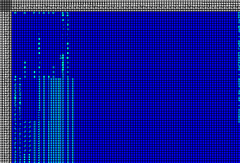
Basics of How to Read this Diagram
Shown is an compile for an XCV300 chip which consists of an
2*48 x 2*32 element array of LUTs. These are
numbered at top and left as numbers 0..47 (column) or 0..31 (row) and
subnumbered L/R (left and right) or F/G. This is how Xilinx numbers them,
due to the way the FPGA chip is wired internally. It consists of 48 x 32
CLBs (configurable logic blocks) of each 2x2 LUTs. Every
F and G pair of LUTs is called a slice (L and R being the
2 slices of the CLB). Slices are officially numbered 0 and 1 with 1=left
and 0=right, which is why all the R slices got used.
A LUT (Look Up Table) is an programmable logic
element, that has 4 inputs that are evaluated to generate 1
output. Evaluation consists of regarding the 4 inputs as an 4bit
number (gives range: 0..15) and using that as index into an 16 line
table containing 1 (output) bit per line.
This graphic shows an grid of 4x4 (= 16) pixel graphics
representing the 16 bits of each look up table, bit 0..3 shown at top
left->right, 12..15 at bottom left->right. The actual table values are
also available as listing of place and 16bit hex
number. The Java code that generated them is here.
Different logic functions require different tables to implement
them, which then appear here as different 4x4 patterns. (Groups
of) identical logic functions appear as (groups of) same
patterns.
The programmable wiring from LUT outputs to inputs, and
the facultative register storage elements after each LUT
are not shown.
Basics of This Chip Design
The PDP-10 is an 36bit processor. For each of these data bits an
near identical processing data path is required,
so that they can all be processed at the same time, so it requires
36 identical repeated sets of logic functions.
Due to the way Xilinx wires their FPGA chips, functional
complexity runs left<->right (with some exeptions), and
bit depth repetition runs top<->bottom, with the
LSB at bottom and MSB at top.
I have placed the data path at the bottom of the chip,
using rows 000F..017G. The 36 times repeated indentical functions
appear as vertical (column/slice) lines. The unused columns are due to an
inefficient placing method, mainly because the logic definitions
are hard-wired dependant on L/R slice placing.
Above these 36 rows appear the control circuits that tell
the data path what function it is to do in the present step of execution.
They are placed in the same column as the part of the data path
that they control. The use of only F rows is also due to hard-wired F/G
LUT dependant code.
Relative to the 1st
milestone I at this time decised that I would make an visualisation
tool. So the chip now contains commenting elements. These are the row of
mnemonic characters at the top (to make it easy to point out columns) and
the comment column at the right (to identify the design). Later while
designing the tool I added code for includiong the FPGA addresses, so the
mnemonics have become superfluous.
The actual Data Path Elements
These are described ordered by function and so by column.
- 000R+001R "M": (Test) Memory of 32 words
- Here the logic elements are used as 16bit RAMs, in
pairs to give 32 words space. Allways an F and G LUT pair are one bits
memory (this is one of the complexity left<->right exeptions), giving
only space for 1 bit per 2 rows, so alternating bits
need to be zigzagged between 2 columns, bits 35,33,31,..,1 in
column 000R and 34,32,30,..,0 in 001R. There is no vertical stripe of
identical patterns, as memory content varies for each bit. This
remained the same as in the 1st milestone, appart from containing
an new test program, so the new instructions can also be tested
- 002R+003R "A": Memory Address Multiplexer
- This selects the source to take the current memory
address from, to select an word. Possible selections are:
program counter (PC), memory address register
(MA), instruction register X or AC field (IR.X or
IR.AC). Here also 2 logic elements are required per bit, so there are
also 2 columns. Only 000F..008G are used, as PDP-10 addresses
are only 18bit wide. 000F..001G differ from the rest because
for bits 35..32 the IR.X or IR.AC can be used, while for 31..0 an 0 is
inserted (extension of 4bit addresses to 18bit). This remained the
same as in the 1st milestone
- 004R "P": Program Counter (PC)
- This is a 18bit (only 000F..008G) register (invisible) that stores
and provides the memory address for fetching the
next instruction (1 word of 36 bits). Visible is the
logic for generating the next instruction address. This is a
adder for calculating
nextPC = oldPC+1 and a
multiplexer for selecting the adder ("normal": use
next instruction and "skip" 2 times next instruction) or the MA
register ("jump": use address in instruction). Relative to the 1st
milestone this got added the ability to be double-triggered
for skip increment
- 005R "I": Instruction and Memory Address Registers (IR+MA)
- These are 2 (invisible) 18bit registers and their visible loading
logic, that are loaded with the 2 halves of the current
instruction. MA (000F..008G) gets the Y address
part (bits 35..18) and can be after modified by index
additions and indirect address loads. IR
(009F..017G) gets the actual instruction (bits 17..0).
Of IR the bottom 4 bits (17..14) are IR.X, which gets
deleted after index calculation and reloaded on index dereferrence, so
they require different logic. The next bit (13) is IR.I
, which only gets reloaded on index dereferrence, requiring
yet different logic. The large control circuits section at the top is
the basic state machine for driving the load, index,
indirect, execute cycle. Relative to the 1st milestone this section
was entirely redesigned for simpler code and for visible
difference of differently behaving elements
- 006R "A": Arithmetic Register (AR)
- This is a 36bit register (invisible) and its visible loading "logic"
(actually non-logic as it simply passes trough data from memory).
This register is used by instructions that take 2 memory words as
input, to hold the first memory word while the second
memory word is being fetched. Relative to the 1st milestone this
section was entirely replaced, as there is now no central AR
any more, as each instruction unit gets its own AR for higher speed.
So no need for writing back to this AR, nor for the loading
multiplexer
- 007R "I": Immediate Multiplexer
- This selects where some instructions take one of their operands from.
Possible selections are: MA register (zero extended, which
gives the visible 18/18 spilt), or the AR temporary register (which
has in it the first memory word, addressed by MA, from the last time
step). This part is used for all instructions which have Memory
and Immediate variants. Relative to the 1st milestone this
section is totally new, allowing using MA as immediate without first
transfering it to AR, so saving one time step
- 008L+008R+009L+009R "W": Memory Data Write Multiplexer
- This selects where to take data from, to write to memory. Because
each instruction unit has its own AR, this is needed to select which
of the 8 instruction groups ARs can send to memory.
This is a large 8-input multiplexer, so it takes up 4 logic
elements per data bit. Relative to the 1st milestone this section
is totally new, allowing multiple unit ARs, for higher speed
- 010L+010R "3 (sort of)": Arithmetic Testing Instruction Unit
- This implements the 011tttmmm arithmetic testing
instructions. There are 2 entirely different logic elements per bit.
010R does the actual arithmetic (Acc-Mem|Immed for CAM|CAI,
Acc|Mem-0 for JUMP|SKIP, Acc|Mem+1 for AOJ|AOS, Acc|Mem-1 for SOJ|SOS).
010L compares the arithmetic result with zero for testing for
E/LE/N/G jump/skip conditions. The "bulge" into 010L in the control
section is the circuit to do the condition evaluation. The "3"
mnemonic at the top got overwritten by too much logic for the wastive
dumb placing method. Relative to the 1st milestone this section is
totally new, doubling the implemented instruction count (1/8th to now
2/8th)
- 011R+012R "4": Boolean Logic Instruction Unit
- This implements the 100ffffmm boolean logic
instructions. These 16 instructions (SET*, AND*, XOR, IOR, EQV, ORC*)
all work by providing a pattern of 4 bits (ffff) and having the 2 data
bits select from them. This is done by an 4-input multiplexer
realised in 2 logic elements/columns. The 4 modes
(Basic, Immediate, Memory, Both) are just different
memory address selections, which are done by the control
logic above this column. This remained the same as in the 1st
milestone
- 047R: Revision Text
- This allows identifying the design from its picture. It lists
Filename - Author - Compile Date - Target Chip. Relative to the 1st
milestone this is totally new
Home |
Projects |
PDP-10 FPGA clone | Chip Layout Description
This page is by Neil Franklin, last modification 2002.10.29