Home |
Projects |
PDP-10 FPGA clone | Chip Layout Description
PDP-10 FPGA Clone Chip Layout Description
This is a description of the design and layout of the FPGA PDP-10 clone
microprocessor.
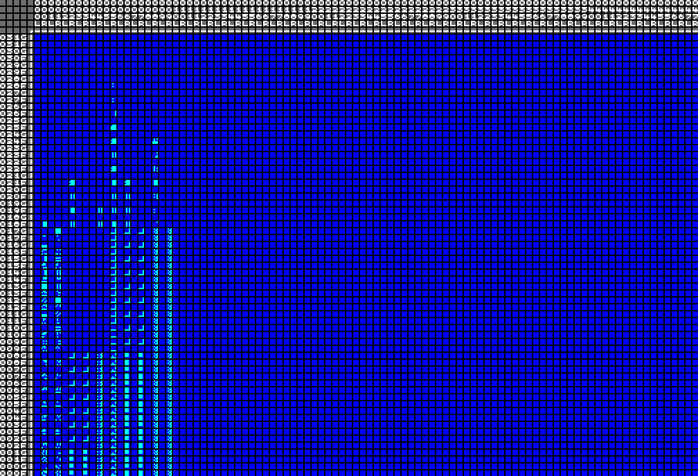
Basics of How to Read this Diagram
Shown is an compile for an XCV300 chip which consists of an
2*48 x 2*32 element array of LUTs. These are
numbered at top and left as numbers 0..47 (column) or 0..31 (row) and
subnumbered L/R (left and right) or F/G. This is how Xilinx numbers them,
due to the way the FPGA chip is wired internally. It consists of 48 x 32
CLBs (configurable logic blocks) of each 2x2 LUTs. Every
F and G pair of LUTs is called a slice (L and R being the
2 slices of the CLB). Slices are officially numbered 0 and 1 with 1=left
and 0=right, which is why all the R slices got used.
A LUT (Look Up Table) is an programmable logic
element, that has 4 inputs that are evaluated to generate 1
output. Evaluation consists of regarding the 4 inputs as an 4bit
number (gives range: 0..15) and using that as index into an 16 line
table containing 1 (output) bit per line.
This graphic shows an grid of 4x4 (= 16) pixel graphics
representing the 16 bits of each look up table, bit 0..3 shown at top
left->right, 12..15 at bottom left->right. The actual table values are
also available as listing of place and 16bit hex
number. The Java code that generated them is here.
Different logic functions require different tables to implement
them, which then appear here as different 4x4 patterns. (Groups
of) identical logic functions appear as (groups of) same
patterns.
The programmable wiring from LUT outputs to inputs, and
the facultative register storage elements after each LUT
are not shown.
Basics of This Chip Design
The PDP-10 is an 36bit processor. For each of these data bits an
near identical processing data path is required,
so that they can all be processed at the same time, so it requires
36 identical repeated sets of logic functions.
Due to the way Xilinx wires their FPGA chips, functional
complexity runs left<->right (with some exeptions), and
bit depth repetition runs top<->bottom, with the
LSB at bottom and MSB at top.
I have placed the data path at the bottom of the chip,
using rows 000F..017G. The 36 times repeated indentical functions
appear as vertical (column/slice) lines. The unused columns are due to an
inefficient placing method, mainly because the logic definitions
are hard-wired dependant on L/R slice placing.
Above these 36 rows appear the control circuits that tell
the data path what function it is to do in the present step of execution.
They are placed in the same column as the part of the data path
that they control. The use of only F rows is also due to hard-wired F/G
LUT dependant code.
The actual Data Path Elements
These are described ordered by function and so by column.
- 000R+001R: (Test) Memory of 32 words
- Here the logic elements are used as 16bit RAMs, in
pairs to give 32 words space. Allways an F and G LUT pair are one bits
memory (this is one of the complexity left<->right exeptions), giving
only space for 1 bit per 2 rows, so alternating bits
need to be zigzagged between 2 columns, bits 35,33,31,..,1 in
column 000R and 34,32,30,..,0 in 001R. There is no vertical stripe of
identical patterns, as memory content varies for each bit
- 002R+003R: Memory Address Multiplexer
- This selects the source to take the current memory
address from, to select an word. Possible selections are:
program counter (PC), memory address register
(MA), instruction register X or AC field (IR.X or
IR.AC). Here also 2 logic elements are required per bit, so there are
also 2 columns. Only 000F..008G are used, as PDP-10 addresses
are only 18bit wide. 000F..001G differ from the rest because
for bits 35..32 the IR.X or IR.AC can be used, while for 31..0 an 0 is
inserted (extension of 4bit addresses to 18bit)
- 004R: Program Counter (PC)
- This is a 18bit (only 000F..008G) register (invisible) that stores
and provides the memory address for fetching the
next instruction (1 word of 36 bits). Visible is the
logic for generating the next instruction address. This is a
adder for calculating
nextPC = oldPC+1 and a
multiplexer for selecting the adder ("normal": use
next instruction) or the MA register ("jump": use address in
instruction)
- 005R: Instruction and Memory Address Registers (IR+MA)
- These are 2 (invisible) 18bit registers and their visible loading
logic, that are loaded with the 2 halves of the current
instruction. MA (000F..008G) gets the Y address
part (bits 35..18) and can be after modified by index
additions and indirect address loads. IR
(009F..017G) gets the actual instruction (bits 17..0).
Of IR the bottom 4 bits (17..14) are IR.X, which gets
deleted after index calculation, so they require different logic. The
reload of bits 17..13 on indirect addressing does not show
visibly. The large control circuits section at the top is the basic
state machine for driving the load, index, indirect,
execute cycle
- 006R+007R: Arithmetic Register (AR)
- This is a 36bit register (invisible) and its visible loading logic.
This register holds the intermediate data while
computation, before sending it back to memory (or accumulator). The
loading logic is a multiplexer that selects where to
load from. Possible selections are: MA register (zero extended
, which gives the visible 18/18 spilt), memory data output, or
result of Logic unit below. This also requires 2 logic
elements per bit and is so zigzagged though 2 columns
- 008R+009R: Boolean Logic Instruction Unit
- This implements the 100ffffmm boolean logic
instructions. These 16 instructions (SET*, AND*, XOR, IOR, EQV, ORC*)
all work by providing a pattern of 4 bits (ffff) and having the 2 data
bits select from them. This is done by an 4-input multiplexer
realised in 2 logic elements/columns. The 4 modes
(Basic, Immediate, Memory, Both) are just different
memory address selections, which are done by the control
logic above this column
Home |
Projects |
PDP-10 FPGA clone | Chip Layout Description
This page is by Neil Franklin, last modification 2002.10.29